


- Oxidation Industry solutions
- DE wall panel oxidation regeneration process flow
- DE wall panel oxidation regeneration process
- Service History
- Open Mask Industry Solutions
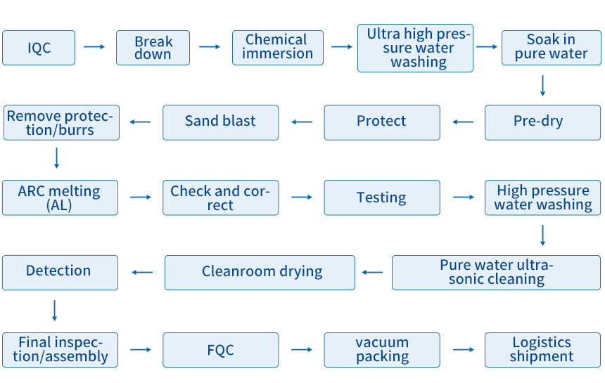
- Open Mask Operation process
- QC Flow Chart
- Open Mask Cleaning Process Flow
- Open Mask Cleaning specifications
- Cleaning specifications
- Semiconductor Industry Solutions
- Photovoltaic cleaning and regeneration process flow - carrier board
- Process flow of semiconductor component cleaning and regeneration
- Ceramic Melting Industry Solutions
- DE Ceramic Component Cleaning and Regeneration Process Flow
- DE Ceramic Component Cleaning Process
- Service History
- Surface treatment process flow of components
- Introduction to Ceramic Melting and Spraying
- Ceramic melting business
- Product Display (Optoelectronics)
- Product Display (Semiconductor)
- Product Display (Semiconductor ESC)
- Ceramic melting technology module
- Ceramic melt blown derivative process (stripping technology)
- Ceramic melt blown derivative process (new oxidation process)
- Surface treatment process flow of components
- Performance testing of oxidation new process performance indicators
- Ceramic melt blown derivative process (cleaning and regeneration process)
- Surface treatment process flow of components
- leaning and regeneration technology capability
- Special product (power on processing)
- Service History
- Cleaning industry Solutions
- PVD component cleaning and regeneration process flow
- Service History
- CF component cleaning and regeneration process flow
- IMP cleaning process flow
- Service History
- Process flow for cleaning and regenerating inner lining components
- Service History
- Quality control capability
- Cleaning and regeneration technology capability
- Advantages of advanced process precision cleaning
- Photovoltaic cleaning and regeneration process flow - carrier board
- CVD Industry Solutions
- CVD component cleaning and regeneration process flow - Diffuser
- CVD component cleaning and regeneration process flow - Baking Plate
- CVD component cleaning and regeneration process flow 1-Susceptor
- CVD component cleaning and regeneration process flow 2-Susceptor
- CVD component cleaning and regeneration process flow - Shadow Frame
- Core technology
- Service History

☆ 2500 square meters of production and service area
☆ Monthly cleaning capacity for 10000 components
☆ Possess complete process capabilities to serve the cleaning, melting, sandblasting, maintenance and refurbishment, precious metal recycling and other needs of 8 "and 12" production lines
☆ It has 2 copper cleaning lines and 2 non copper cleaning lines, including the following processing programs:
1. Chemical peeling and physical peeling
2. Aluminum melting/ceramic melting surface treatment, surface sandblasting, clean room
3. Final cleaning and vacuum packaging
4. Design and production of specialized transport boxes
5. Archive and control of documents related to the use of components
Composition of semiconductor cleaning operation team
|
Consist of |
Staff |
Experience |
|
Technical research and development |
2people |
More than 15 years of experience in the semiconductor cleaning industry |
|
Fusion technology |
1people |
More than 15 years of experience in the semiconductor cleaning industry |
|
Quality Control System |
2people |
More than 15 years of experience in the semiconductor cleaning industry |
|
Manufacturing management |
3people |
More than 15 years of experience in the semiconductor cleaning industry |
|
Sales service |
2people |
More than 15 years of experience in the semiconductor cleaning industry |
① Incoming inspection
Develop a process flow form for the components, inspect the appearance of the components, and report any defects.
② Mask protection
Before chemical film removal, protect the areas that do not require chemical treatment to avoid unnecessary corrosion.
③Chemical membrane removal
Use different ratios of chemical solutions to remove the film layer according to different devices, membrane materials, and materials. Control the use and replacement of chemical agents.
④ Mask protection
Use fixtures or protective tape to mask areas that do not require sandblasting treatment.
⑤ sand blast
According to the requirements of the homework sheet, adjust the sand particle size and spray pressure to ensure that the process set roughness SPEC is achieved.
⑥ ARC melting
ARC arc melting meets the roughness requirements of semiconductor PVD process parts and extends customer PM life time.
⑦ Plasma melting
Plasma plasma spraying forms a Y2O3/Al2O3 coating layer, which slows down component corrosion caused by various plasma gas environments and extends customer PM life time.
⑧ High temperature baking
Using high temperature to gasify surface pollutants of parts, there is no risk of chemical residue on the surface of the parts.
⑨ CO2 micro particle jet cleaning
The use of dry ice particles to impact the surface of components has achieved the goal of removing surface pollutants, which is a green and non-destructive physical cleaning method.
⑩ Correct
Repair the surface of sandblasted and fused parts.
⑪ Inspect
Inspect the flatness, roundness, aperture, roughness, etc. of the repaired components to achieve the work order SPEC.
⑫ AOI detection
Perform aperture and displacement detection on high-precision parts.
⑬ High pressure water washing
Clean the surface of sandblasted and fused parts to remove large particles on the surface.
⑭ Ultrasonic cleaning
Ultrasonic vibration cleaning is performed in a clean room to remove surface particle particles.
⑮ Soda gun rinse/blow dry
Surface particle particles, residual moisture.
⑯ Dry
Class 100 dust-free oven dries the components to ensure complete removal of moisture.
⑰ Final inspection
Appearance inspection, particle inspection, fixture inspection, size inspection, darkroom inspection to ensure that the shipping parameters of the parts are within the standard control range.
⑱ Vacuum packing
Vacuum package the inspected parts according to customer requirements.
⑲ Delivery to customers
The system generates product shipment reports and lists, and delivers them to customers after packing is completed.

Phone: 021-59228356
Address: 1A301, Liandong U Valley, No. 405 Tuoqing Road, Qingpu District, Shanghai


Copyright: Yingyou Optoelectronics Technology Group Co., Ltd. Anhui ICP Registration No. 00000000 Disclaimer
Technical Support: NetEase Technology